CIRCUIT BOARDS OVERVIEW
Technology information, important downloads, interesting special technologies, the right contacts and your advantages at LeitOn.

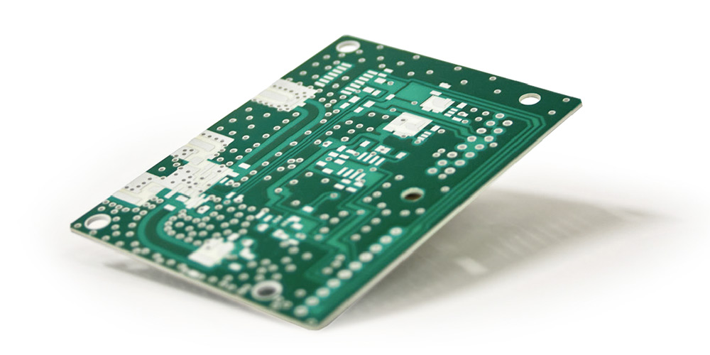
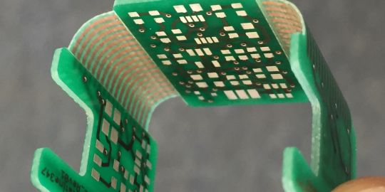
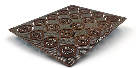
FR4 Rigid printed circuit board | PCB | Tg 150 | Multilayer

FR4 printed circuit boards PCB (multilayer up to 40 layers)

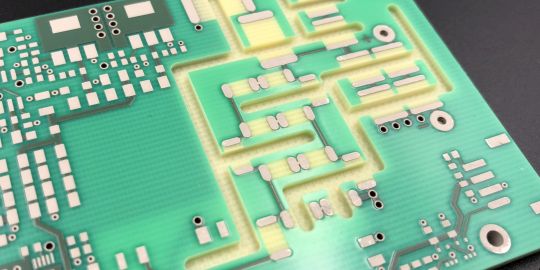
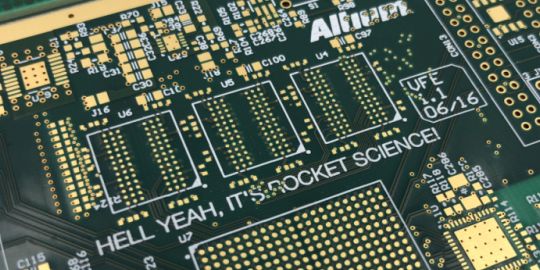
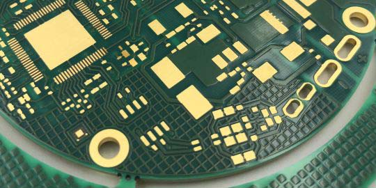
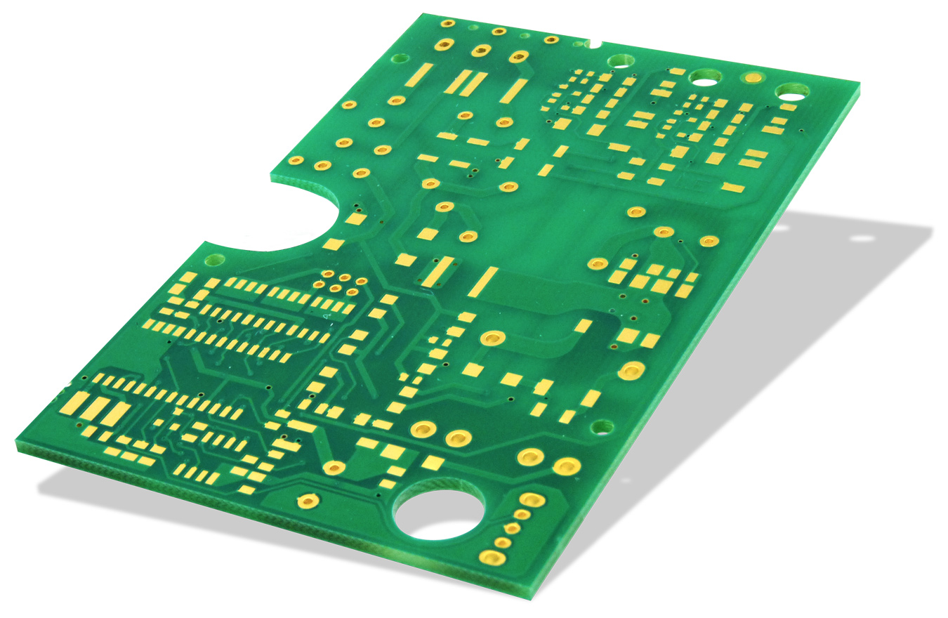
Rigid circuit boards with that certain "extra"

Plating prototype printed circuits

"PCBs aren't just another item on your BOM."

This sentence should immediately make sense to anyone in the electronics industry. Because while most components come “off the peg” in millions of pieces, printed circuit boards are always manufactured individually for the projects. At the same time, they form the carrier and the connecting piece between all other components. The printed circuit board is what all makes electronics “play” in the first place.

We are always aware of this immensely important, central role of the printed circuit board (PCB) in terms of reliability and quality, knowing full well that the production has its individual challenges every time. Careful advice, planning and production are the three cornerstones of printed circuit board production, so that even highly complex special technologies are successful.

Industrially manufactured quality circuit boards

Drill-routing double-head with camera system

LeitOn offers you a wide range of high-quality printed circuit board technologies and options for order processing and logistics.

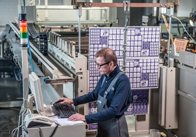
With locations in Germany and China, we can produce any required volume, from express prototypes to mass production, and successfully bring your samples into series production. A large team of experts in the areas of technology, quality, logistics, production and sales is personally at your side to implement and follow up your requirements.

In addition to the usual "make to order" processes, we specialize in a wide variety of logistics agreements for optimal delivery readiness such as call-off stock, consignment stock, sea-air split delivery of series and flexible framework agreements.

Contact persons
Igor Sandara
Technical Sales
+49 (0)30 701 73 49 24
Sascha Kappel
Technical Sales
+49 (0)30 701 73 49 26
Mario Gehrau
Technology Manager
+49 (0)30 701 73 49 20
Technology
for rigid circuit boards

Options

Show all details

Material propertiesTG130, TG150, TG170, (TG250 - no FR4), halogen-free, black FR4
Material manufacturersPanasonic, Isola, Ventec, ShengYi, ITEQ, King Board, NanYa...
Material thicknesses0,1 mm to 4,8 mm
Maximum PCB sizeGermany 508 x 572 mm2, China 1/2-layer 530 x 606 mm2, multilayer 516 x 592 mm2, oversized PCBs on enquiry
Copper thicknesses18µm / 35µm / 55µm / 70µm / 105µm / 140µm / 210µm / 300µm / 400µm
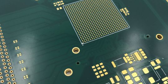
Layer count1 to 40 layers
Surface finishesHAL-lead-free, HAL, ENIG, ENEPIG, immersin tin (iSn), immersion silver, OSP, connector-gold
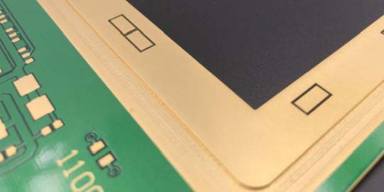
Mechanical machiningrouting, milling, scoring, jump scoring, chamfering, semi-flex, depth milling, countersinking, punching
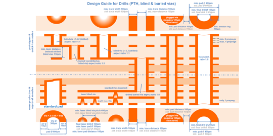
Drill optionsMicro-vias, blind-vias, laser-vias, stacked-vias (SBU), press-fit
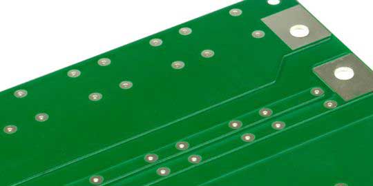
MetallizationsEdge metallization, stamp-outlines, half-opens, oblong holes, metallized slots, metallized depth milling
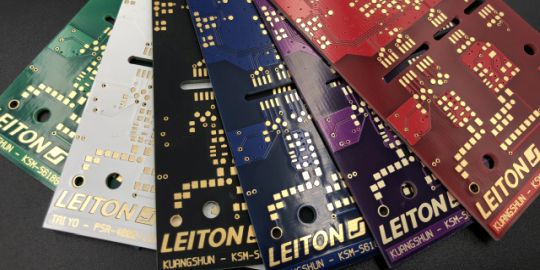
Solder maskLacquer, flex lacquer, coverlay. Lacquer colors: green, black, red, blue, yellow, white, special colors (all RAL colors) and matt lacquers
Special printsPeelable lacquer, carbon printing, UV reflection lacquer, silk screen printing
Special technologies2mil structures, coils, frame technology, prepreg or core pressed on one side, FR4-Flex, 3M on FR4, LP numbering, special layer structures, impedance measurement, plugging, filling & tenting, copper VIA filling
Quality Management & CertificationsISO 9001, ISO 14001, UL, IPC2/IPC3, IATF 16949, EMPB, VDA2, PPAP, cross-sections (x-sections), measurements, declarations of conformity, data sheets, ESD packaging and more
LogisticsFramework orders, consignment stock, call-off stock, sea-air split orders, express delivery from 2 working days
Special technologies
Rigid circuit boards (FR4, Rogers, High-TG)

Read more
LeitOn GmbH has specialized in cost-effective hybrid solutions that only use expensive RF materials where they are actually needed. The rest remains a conventional FR4 multilayer and therefore cost-effective.
Read more
Calculate now
For printed circuits under extreme power conditions, copper thickness of 70µm, 105µm up to 140µm is available for mass production. Prototypes can be produced with copper thickness up to 400µm thick. These copper thicknesses are also available as inner layers so that you can realize solid high-power multilayer-PCB applications.
Read more
Most FR4 printed circuits can be easily converted into so called semi-flex PCBs. By reducing some areas to a thickness of only 200µm +/-50µm by z-axis routing, these areas become slightly flexible. Flexible enough for so called flex-to-install applications. To avoid solder mask breaking off, a special flex solder mask is applied.
Read more
Calculate now
For sensitive high-frequency applications critical impedances can be planned, controlled and measured so that you will only receive PCBs with the requested impedance characteristics. The calculation can be bought from us in advance so that you have all stack-up and material information available early on in your project.
Read more
Calculate now
Special routing or milling outlines with toolings down to 0,7mm diameter are common. Usually, such routings are included in the standard price. High tolerance requirements can be incorporated, measured and documented if they are critical to your application. For special purposes we can also use flat-head tools or other equipment.
Read more
For seamless installation with screws we can add countersink drills into your printed circuit board. Screws will not be visible from the side after installation. Depending on your requirements we can offer a range of different diameters and angles. Please note that additional costs for this countersink process do incur.
Read more
Calculate now
If certain areas on the printed circuit must be protected from hot solder wave in some steps, we can cover them with peelable mask on your printed circuit. This peelable mask will protect the area and can be easily removed afterwards. Peelable mask does not leave any residues and the surface underneath remains ready for soldering.
Read more
Calculate now
For light-sensitive sensors black solder mask is often not sufficient to block light out. For such requirements we can offer black FR4 material, which is completely opaque and will not let any light diffuse through the PCB. Due to its practical use in the industry it is available for mass production and prototypes.
Read more
Keyboards and buttons with partial carbon ink on the PCBs prolong abrasion resistance and are a cost-efficient alternative to hard gold plating. But keep on mind that some design rules must be followed, because the carbon ink is initially liquid when applied and flows slightly on the circuit board before curing.
Read more
Calculate now
Standard Rogers 4003C or 4350B materials, and the new 4360G2 are on stock for prototypes and mass production in a wide range of thicknesses. Hybrid stack-ups for multilayers with FR4 and Rogers materials can be produced, too. Impedance measurements at the end of production can assure that the actual printed circuits fulfil your requirements.
Read more
Quality assurance is one thing, documentation another. We understand the need for certainty and can offer extensive documentation of a wide range of individual measurements, according to your needs. Apart from cross-sections and initial sample inspection and impedance reports we can measure individual tolerance requirements.
Read more
Calculate now
Hard gold thicknesses of 0,5µm to 0,8µm are common for mass production, for prototypes we can produce up to 3µm hard gold. Gold prices can become a real cost driver here. We happily consult you on the application requirements and accompany you with some evaluation cycles in order to determine the optimum gold thickness.
Read more
Plated outlines for printed circuit boards are possible. You can partially plate outlines or even almost the entire PCB, so that after separation only the panel connections have no plating. Plated outlines usually require small surcharges, while plated slots, which are located somewhere within the PCB area, are commonly included in the price.
Read more
For contacting your printed circuits from the sides we can offer half-open PTH drills. Production of this type of PCB looks simple but it is not. Because simply milling through the PTH at the end of the process would destroy all copper walls, the process involves several mechanical drilling and routing steps around the actual plating process.
Read more
Z-axis milling on PCBs can be produced in a range of widths and depths. Milling can be done as channels or even complete areas can be "lowered" down. Depending on the requirement we can use normal tools or flat-head milling tools which will provide a more even/flat surface, just like semi-flexible printed circuits are produced.
Read more
Calculate now
High-TG PCBs with TGs of 150°C, 170°C or even up to 260°C can be offered in a wide range of thicknesses and copper weights. Apart from the obvious advantage regarding temperature performance, high-TG materials also tend to warp less and are therefore preferred materials when it comes to assembling large and complex PCBs.
Read more
Plating the z-axis milling with copper on the printed circuit board is also possible. You may for example solder a flange into such a milled and plated z-axis or protect contact areas better. We successfully produced hard-gold-plated z-axis areas to move abrasive contacts below the PCB Top-layer surface level.
Read more
Calculate now
Today red, blue and purple are as common as green, white or black. Many colors are available in matt. If you like to create your own color, keep in mind that such individual colors require minimum order quantities and are therefore often only economically viable for larger quantities. We do keep a wide range of different solder mask color PCBs, ask us for samples.
Read more
Calculate now
Regardless of any later impedance measurement or if you prefer to produce the PCB at another supplier, we do offer you full and professional impedance calculation in advance. We will calculate the stack-up and the required trace width/gap as well as the materials. By doing this early on one can be sure that the actual layout will be producible.
Plugging stands for closing plated through holes and then applying a copper-lid that covers it. You will not only have the hole closed but a copper-pad on top of it which can accommodate a normal soldering process just like any pad. This technology is especially important when the printed circuit board contains BGA components.
Read more
Calculate now
Blind vias can be an efficient way to keep the printed circuit board dimensions small. Alternatively, one would have to apply a clearance to these drills in all layers where they do not contact anything and lose this space for routing traces. Although blind vias require a surcharge, it might therefore still be an economically viable choice. If there is even less space, laser vias may be an option.
Read more
Calculate now
Connector gold is an electrolytic hard gold with cobalt, which makes the contacts more resistant against abrasive forces. Such hard gold is recommended for connectors with many connection cycles. Additionally, we recommend beveling for smoother connector insertion. Connector gold usually ranges between 0,5µm and 1,2µm hard gold.
Read more
SBU stands for Sequential Build-Up and classifies multilayer-PCBs which are not laminated in one single process but consist of several multilayers that are sequentially build together step by step. SBUs are mostly used when vias or blind vias have extreme aspect-ratios which can be made feasible thanks to this SBU process.
Read more
Calculate now
Multilayers with up to 24 layers can be produced as quick-turn prototypes or are available for mass production. Hybrid stack-up, blind vias, 4mil structures, buried vias and copper-lid plugging for BGA components are possible in combination. Usually, such high-layer PCBs are produced with immersion gold finish (ENIG or ENEPIG).
Read more
For some applications applying cover-lay onto the PCB is better than solder mask. Usually, cover-lay is only used for flexible circuits. However, we successfully apply cover-lay on some rigid PCBs, too. The advantages are increased abrasive resistance and higher break down voltage resistance. According to IPC solder mask is not allowed as an electric isolator.
Read more
In case each batch or even each single PCB has to be traceable we can accommodate individual IDs on each board or each panel. It is recommended to use DCC codes which are harmonized and can be read by scanners. Depending on the complexity of the required code, such DCC fields only require a small area of the PCB.
Read more
Calculate now
Rigid printed circuit boards are available in an almost seamless range of thicknesses, starting at 0,1mm up to 4,0mm. In combination with different copper weights and special material characteristics such as high-TG or CTI, this amounts to an extensive stock of materials that includes hundreds of different material types.
Read more
Calculate now
For very tight impedance controlled printed circuit boards measuring one or even several representative coupons of the production panel may not be sufficient. If the exact impedance for each PCB needs to be controlled and be known throughout the entire assembly process we can integrate a test coupon onto the panel.
Read more
PDF
Special stack-ups can contain a range of deviations from common printed circuit boards. Different materials can be combined in one stack-up (so-called "hybrids") or asymmetric stack-ups can be built. Even different copper thicknesses throughout the PCB are sometimes possible. We can prepare and send you possible stack-ups in advance.
Read more
PDF
Depending on the country of production, there are different possibilities and restrictions for drilling. For example, laser drilling is not possible everywhere. Mechanical blind holes, on the other hand, also offer their advantages. You can find out what needs to be considered when designing holes by downloading our design guide PDF.
Our circuit boards in detail

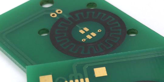
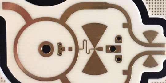
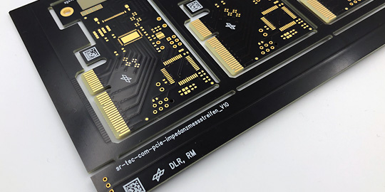
Materials & properties of FR4

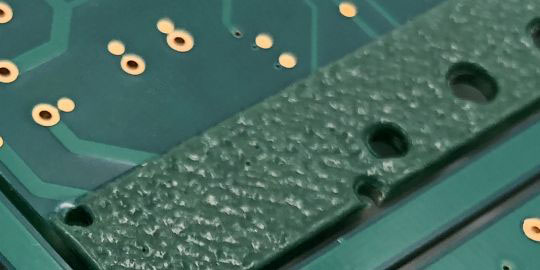
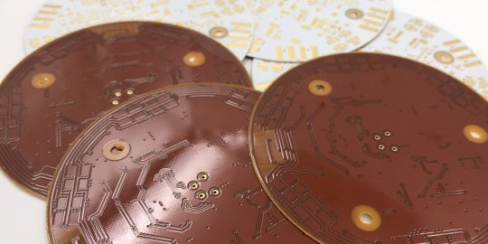
FR4 material is rigid and has become the standard material for printed circuit boards, compared to older materials like Pertinax, FR1 or CEM1. “FR” stands for “flame-retardant” and has a UL classification of 94V0. In the case of rigid-flex circuit boards, it forms the stable part on which components can be assembled. A popular low-cost way to make FR4 boards partially bendable is the so-called "semi-flex", where areas are simply depth-milled to achieve a certain flexibility. Common manufacturers for FR4 base materials are ISOLA, Panasonic, Kingboard, Shengyi and Nanya.

Materials of FR4 printed circuit boards

FR4 base material consists of the materials epoxy and a woven glass fiber fabric. Modern circuit board material has various fillers, which are usually required for higher temperature resistance. However, this makes the circuit board material a bit more brittle and high-TG-FR4 >150°C is therefore only of limited use for Semi-Flex. Copper is rolled-annealed onto the substrate as a conductive material.

Temperature resistance of FR4

The usual temperature resistance of FR4 is 130°C (TG130). For multilayer boards, a TG150 material is usually used as the standard, as such material expands less in the Z direction when heated and therefore allows more stable vias (PTH). High TG170 or TG180 material is used for very warm environments. TG210 materials are very rare and even higher TGs are currently not achievable with FR4, but you have to switch to polyimide or other materials. TG means “glass transition temperature”, i.e. the temperature at which the material becomes soft. The operation temperature should therefore not exceed TG minus 25°C.

MaterialDesignationOperating temperatureMaterial type
TG130Low-TGca. 110°CFR4 (Epoxy-fibre-glass)
TG150Mid-TGca. 125°CFR4 (filled epoxy-fibre-glass)
TG170High-TGca. 145°CFR4 (filled epoxy-fibre-glass)
TG250Ultra-High-TGca. 220°CPolyimide or ceramics

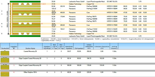
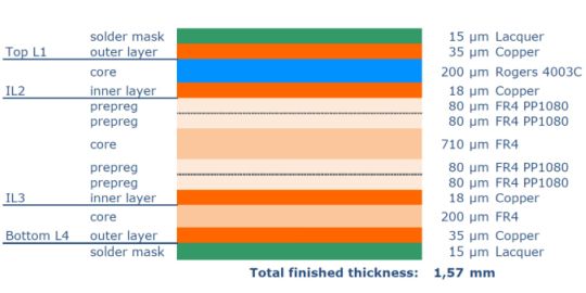
Layer structure & standard thicknesses

The standard thickness of FR4 circuit boards is 1.6mm and 1.5mm respectively. Thin rigid base materials go down to 0.1mm or 0.2mm. A thickness of 2mm is a common choice for sturdier, larger boards. Copper thicknesses are based on an American system of "Oz/ft2", i.e. "ounce per square foot". One ounce (1 oz) of copper per square foot corresponds to approximately 35µm of copper thickness. We often speak of 1 oz, 2 oz (70µm), 3 oz (105µm) when the copper thickness is meant. Starting copper before electroplating is usually around 18µm (1/2 oz). The origin in the American system explains the crooked standard values in the metric system.

The layer structures for multilayers differ significantly depending on the manufacturer and material manufacturer.

Typical layer stack-up for 4-layer multilayer

An overview of the respective standard layer structures of various thicknesses and numbers of layers can be found here as a PDF download.

Electric strength

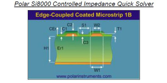
For high voltages it is important that the layers of a printed circuit board insulate sufficiently from each other. A parameter for this is the dielectric strength, which is specified in every data sheet under "Electrical Strength" in kV/mm (kilo-volts per millimeter). The IPC-TM-650 Chapter 2.5.6.2 requires at least 30kV/mm here. Common FR4 materials usually achieve 40-50kV/mm or even more.

You can find an overview of filter functions for various properties in our base material database.

Preview of LeitOn’s base-material-finder

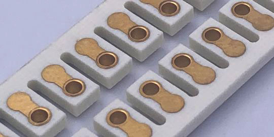
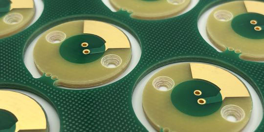
FR4 printed circuit boards (PCB)

PCB is the English abbreviation for "printed circuit board". Circuit board prototypes are already very cheap today, which is why the breadboards used in the past are not common anymore. Also, such hole grids are only suitable to a very limited extent for the assembly of SMD components, which are increasingly dominating electronics.

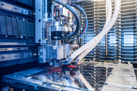
The production of our printed circuit boards

The manufacturing process of printed circuit boards is largely identical in all common productions. It can be roughly divided into mechanical, chemical and photo-sensitive processes, with industrially manufactured circuit boards moving back and forth between these process fields several times during production. A detailed circuit board production process is available for download here. The individual process steps for production are briefly explained here.

Buy cheap PCB prototypes online directly from manufacturer

At LeitOn we offer cheap PCB prototypes in the online calculation or on request. A large selection of material is already available online, as well as various options regarding the number of layers, copper and total thickness, solder mask colors, special prints and finishes. Our prototypes are particularly inexpensive thanks to the “shared production” concept, with different layouts being placed on the same production blank. This saves initial costs and setup and leads to particularly low prices with the best quality.

What our customers say
FAQ
FR4 (or FR-4) is a base material for printed circuit boards (PCB) and consists of composite materials, primarily epoxy resin and glass fiber fabric. FR4 stands for "flame retardant, class 4". Fillers can give FR4 a higher temperature resistance (TG = glass transition temperature). Maximum operating temperatures (MOT) of FR4 material are mostly between 110°C and 150°C.
Printed circuit boards differ significantly in the number of layers (1-layer, 2-layer (through-plated) and multilayer ?4 layers). Furthermore, the type is differentiated: rigid (PCB), flexible (FPC), rigid-flex (RFPCB = rigid and flexible areas on a printed circuit board). Materials are another feature of different types: FR4 (standard), ceramic (for RF applications), polyimide (flexible circuit boards) and aluminum IMS "insulated metal substrate" are just a small selection.
The Tg is an important characteristic of printed circuit boards (PCB) because it indicates the temperature resistance. Tg stands for "temperature of glass-transition", is given in °C and describes the temperature point at which the material becomes mechanically unstable. Usual FR4 material has a of Tg130°C (low-Tg) as standard, for multilayers mostly Tg150°C (mid-Tg) or Tg170°C/Tg180°C (high-Tg) is used. Higher Tg of up to ≈260°C mostly require polyimide or other materials than FR4. The maximum operating temperature (MOT) is approx. 20C° below the specified Tg.
Conventional printed circuit boards require 3 types of processes:
  1. mechanical (M)
  2. chemical (C)
  3. photosensitive (P)

In short, the process of a 2-layer circuit board is as follows:

drilling (M) → through-hole plating (PTH/THP) (C) → laminating & exposing (P) → etching (C) → solder mask & exposing (P) → surface coating (C) → milling (M).

There are also various intermediate thermal processes, tests and cleaning steps.

The specific weight of printed circuit boards (PCB) largely depends on the copper content (copper thickness, number of layers and occupied copper area), since copper has a specific gravity of 8.9 kg/dm³ and FR4 base material only approx. 2.3 kg/dm³. The fact that a printed circuit board usually consists of far more FR4 than copper can be assumed for a standard printed circuit board (2-layer, 1.6mm thick with 35µm copper, 75% covered) of approx. 4 kg/m² printed circuit board area. A circuit board with the above parameters of size 100 x 100 mm² weighs approx. 40g.
The cost of a printed circuit board (PCB) depends on various parameters. In addition to the technical specifications and the urgency (express surcharges), the quantity has an immense influence on the costs. The factor between a prototype and a large series can be many times over here. If a prototype costs e.g. EUR 50, the price in a large series can quickly be far below EUR 1 per piece.
Printed circuit boards (PCB) can be ordered via our online calculation or via e-mail. The prices are identical. The production data must be transferred in a common layout format (Gerber, Eagle, Target, KiCAD, etc.). When ordering, the quantity, desired lead-time and technical specifications (thickness, copper plating, colour, surface finish, etc.) must always be specified.
Printed circuit boards are assembled (PCBA) either by hand or with a machine. The choice of the right process depends on the number of pieces and the components used. For very small quantities, it is sometimes not worthwhile to set up a machine for automatic assembly at great expense. On the other hand, very complex/small components can require automatic assembly, since manual assembly would be too imprecise.
PCB does not stand for a material, but is the English abbreviation of "Printed Circuit Board", i.e. a "printed circuit" or “circuit board”. Typically, a PCB is made of FR4 material. Various electronic components are attached to a PCB, which are connected to one another via conductor tracks made of copper in order to achieve a desired electrical function.
The green color of printed circuit boards (PCB) comes from the so-called solder-stop mask. As the name suggests, solder-stop mask is intended to “stop the solder”. In other words, the green laquer is applied to prevent short circuits when the PCB is soldered. Even if all colors are possible today, most printed circuit boards are still green. There are several reasons for this: on the one hand, green contrasts well with the copper-colored surface. On the other hand, green used to be a dye that was very easy to produce. But why it is still dominant today is due to the good processability in terms of exposure time. Exposure time is optimal for green laquer. Lighter colors reflect the light in this process above average, while dark colors absorb the light very much. Both mean that the exposure times have to be longer and the structures that can be produced are not as fine as with green solder mask.
Climate-neutral operation
since 2021
  • CO2 neutral through compensation
  • Circuit boards – green on the outside, also on the inside
Member of the Fachverband Elektronik-Design
  • Expertise through active exchange
  • Expertise through training and further education
ISO tested by the most renowned auditor in Germany
  • ISO 9001:2015 Quality Management
  • ISO 14001:2015 Environmental Management
UL approvals for various types of circuit boards
  • UL for rigid FR4 PCBs
  • UL for flexible circuit boards
  • UL for aluminum IMS boards